

产品信息
详细介绍
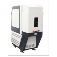
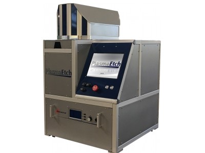
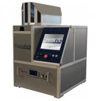
等离子芯片开封机PlasmaEtch
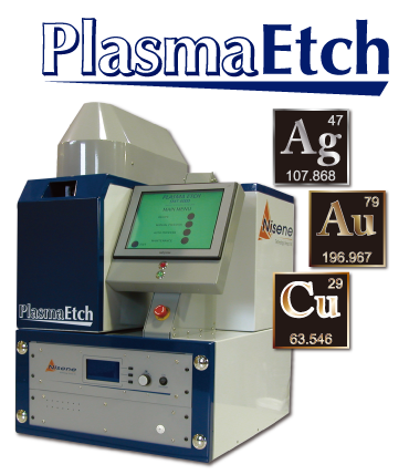
无论是传统的金线样品,还是样品都采用铜线或银线,PlasmaEtch都能提供安全可靠的蚀刻。
 As the world moves toward more eco-friendly processes and the semiconductor manufacturing industry continues to make smaller parts with sensitive internal components, failure analysts are presented with a unique challenge: how do you etch these samples? Nisene Technology Group has bridged the gap between semiconductor manufacturing technology and failure analysis with its latest decapsulation system: the PlasmaEtch.
工作原理:
The PlasmaEtch decapsulation system is a revolutionary patent-pending gas-based semiconductor etching system. Employing a never-before-seen application of microwaved gases inciting chemical radicals for isotropic etching, the PlasmaEtch is the greenest and most cost-effective etching solution available. The PlasmaEtch can etch most sample sizes, encapsulant types, and wire bond types. Whether it’s a more traditional gold wire sample, or if the sample features copper or silver wires, the PlasmaEtch delivers a safe and reliable etch.
PlasmaEtch创新点:
Afterburner Downstream Focused Plasma Etching(延时激发下行聚焦离子蚀刻)
Mass Flow Controlling for All Gases(所有气体流量可控)
No Microwave Radiation Exposure to Samples During Etch Process(无微波辐射)
Low Temperature Etching(低温蚀刻)
Isotropic Etching(等向性蚀刻)

Unlike typical and less sophisticated plasma decap systems that take many hours or even days to get to the surface of the die, the PlasmaEtch can clear the encapsulant of most package types and reveal the complete die surface and wire sweep in a matter of a couple hours. Chemical-free decapsulation has never been so effective.
主要特色(Highlights):
Highly Customizable Etch Recipes(高度可定制的蚀刻配方)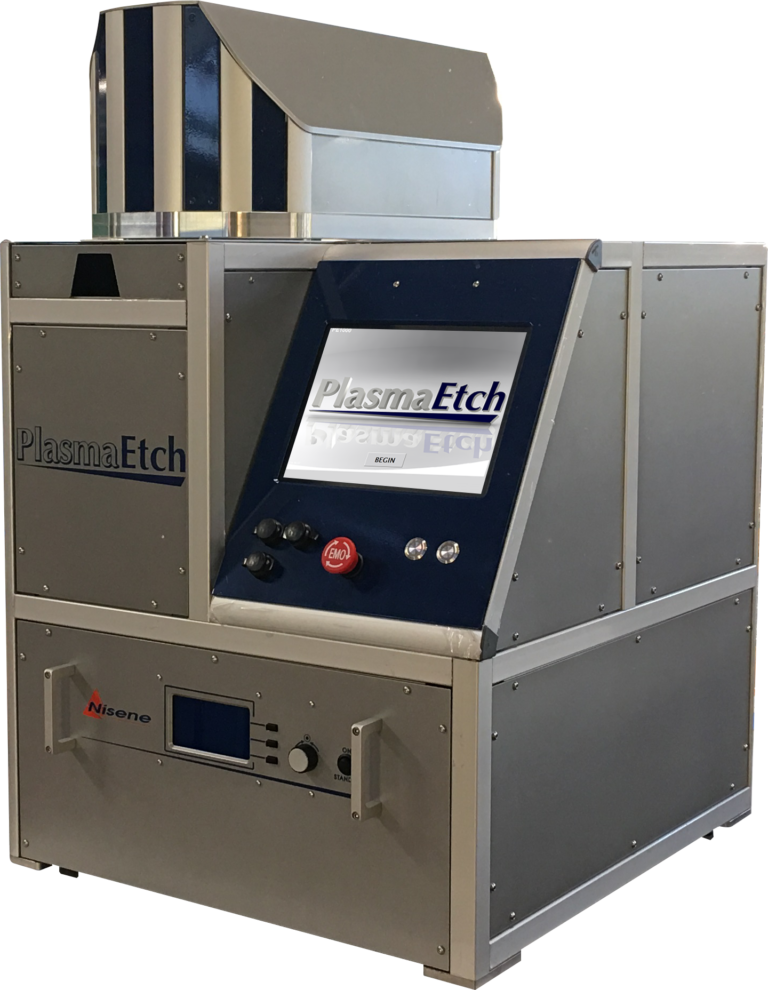
Etches a Wide Variety of Package Types(可蚀刻各种各样的封装类型)
Completely Chemical-free Decap(完全非化学方式蚀刻)
Eco-friendly(生态友好环保)
Touchscreen Interface(触控屏)
PC/Windows-based GUI(基于PC / Windows的GUI)
The only Solution for Silver Wires(银线的唯一解决方案)
Etches Samples with All Wire Types(可蚀刻所有引线类型的样品)
Small Footprint Suited for Tabletop(桌上型紧凑尺寸机柜)
产品优势